IBM 2nm chip claims more power with less energy
The process used to make computer chips is measured in nanometres (nm) – with a lower number usually signifying a leap forward.
IBM claims its test chip can improve performance by 45% over current 7nm commercially available products.
It is also more energy-efficient – using 75% less energy to match current performance, IBM said.
It claims the tech could “quadruple” mobile phone battery life, and phones might only need to be changed every four days.
The computer chip industry used to use nanometres – one billionth of a meter – to measure the physical size of transistors. Today, a lower “nm” number is widely seen as a marketing term to describe new generations of technology, leading to better performance and lower power.
 IMAGE COPYRIGHT IBM
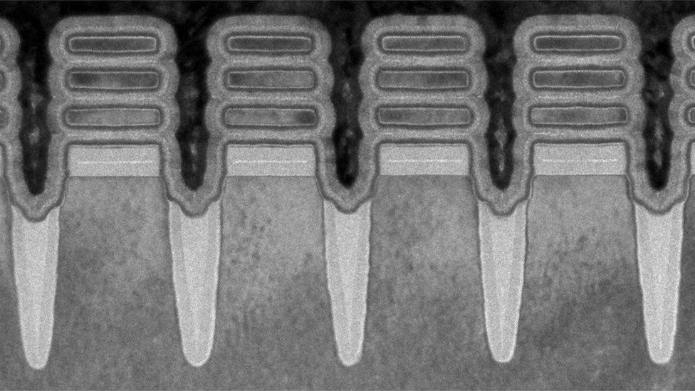
image captionTransistors on the IBM “nanosheet” it uses for the new tech
IBM says its 2nm process can cram 50 billion transistors into “a chip the size of a fingernail” – up from 30 billion when it announced its 5nm breakthrough in 2017.
The end result should be another performance bump for computers in the coming years.
‘A breakthrough’
Current high-end desktop chips based on the 7nm process, such as AMD’s Ryzen processors, did not become widely available until 2019 – four years after IBM announced it had cracked the 7nm process.
But mainstream commercial chip-makers such as Intel and TSMC – which makes AMD processors – have already said they plan to build ultra-low nm chip plants in the next several years.
“This can be considered as a breakthrough,” said Peter Rudden, research director at market intelligence firm IDC.
 IMAGE COPYRIGHT IBM
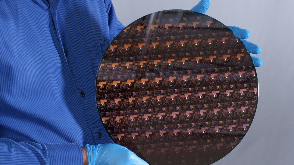
image captionThe chip wafer for the 2nm chip, held by an IBM employee
“We have seen semiconductor manufacturers moving from 14nm to 10nm to 7nm, with 7nm being a real challenge for some,” he explained. He said IBM’s new process could be used for AI uses that today need a second piece of tech – such as a powerful graphics card- to handle some tasks. The increased power efficiency could be useful in personal devices, while increased performance would benefit huge datacentres, he added.
“This also sends a message to the IT industry that IBM continues to be a hardware research powerhouse.”
